
수록 모음: 투자자 발표자료 사례
Applied Materials Investor Breakfast 2026 — the 99-page presentation Applied Materials gave investors at SEMICON West on October 13, 2026, laying out how AI computing is reshaping wafer fab equipment (WFE) demand and setting calendar-2030 financial targets: more than 2 points of WFE share gain, over $12B in services revenue, ~54% non-GAAP gross margin and ~40% non-GAAP operating margin.
빠른 탐색
태그
슬라이드 공유
Applied Materials Investor Breakfast 2026 — the 99-page presentation Applied Materials gave investors at SEMICON West on October 13, 2026, laying out how AI computing is reshaping wafer fab equipment (WFE) demand and setting calendar-2030 financial targets: more than 2 points of WFE share gain, over $12B in services revenue, ~54% non-GAAP gross margin and ~40% non-GAAP operating margin.
레이아웃, 주요 콘텐츠 및 시각적 요소를 포함한 각 슬라이드 페이지의 상세 보기.
Title slide for the Applied Materials Investor Breakfast 2026, held at SEMICON West. The deck introduces the company's AI-driven strategy and 2030 targets.
Centered Applied Materials logo above a white title banner with a cyan '2026' tab, over an abstract blue glass-panel background.
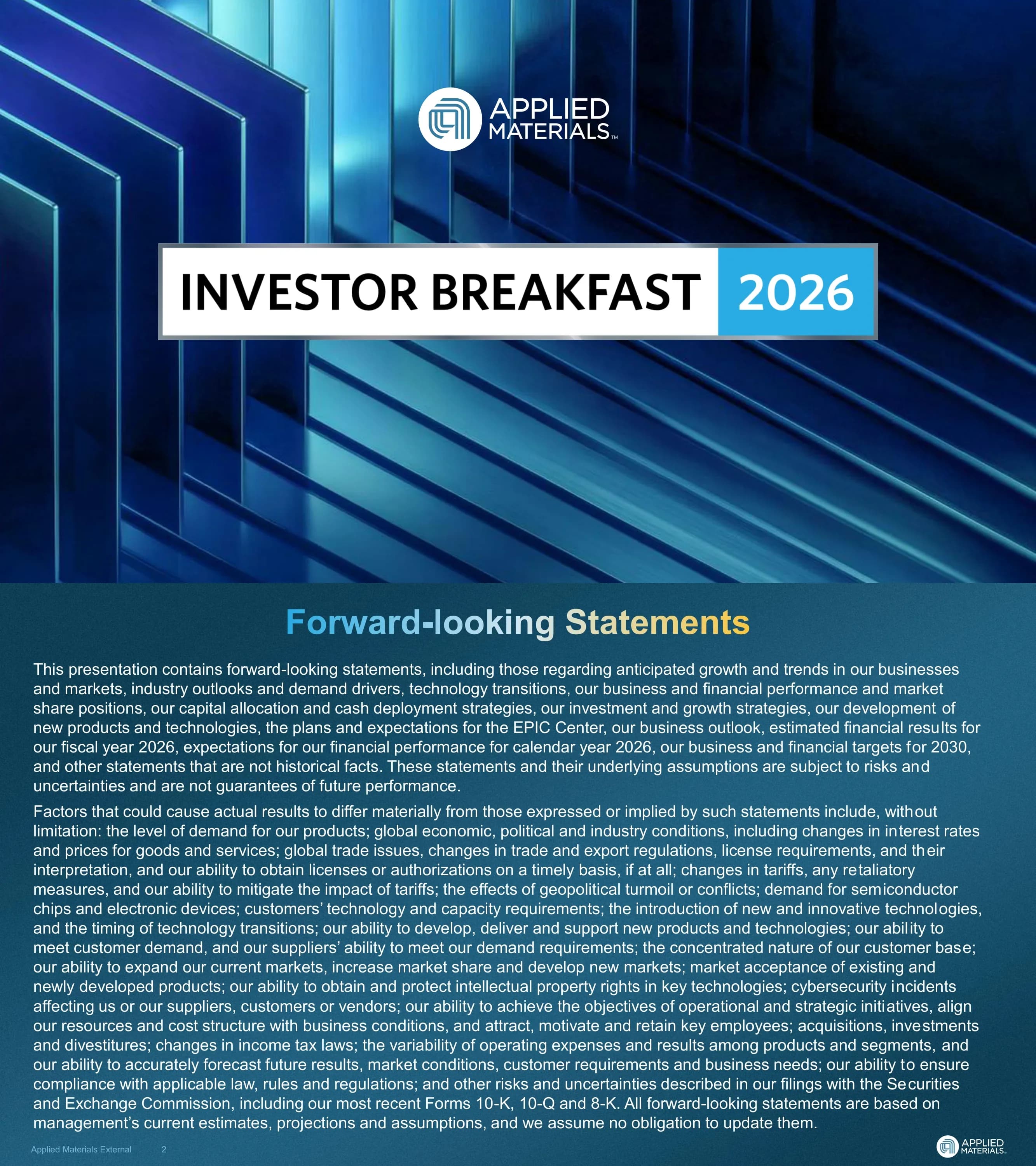
Legal disclaimer stating the presentation contains forward-looking statements on growth, technology transitions, the EPIC Center, fiscal year 2026 results, calendar year 2026 expectations and business and financial targets for 2030. It lists risk factors such as demand, trade and export regulations, tariffs, geopolitics and customer concentration, and refers readers to SEC filings (Forms 10-K, 10-Q and 8-K).
Full-width dense text blocks of two paragraphs under a gradient title on a teal background.
Speaker introduction slide for Mike Sullivan, CVP, Investor Relations, who opens the investor event.
Left-aligned large white name with a job title beneath it over a dark blue abstract panel background.
Morning schedule: 8:05 Strategy + Vision (Gary Dickerson); 8:30 Semiconductor Products Group (Dr. Prabu Raja); 8:55 Imaging and Process Control (Keith Wells); 9:05 Applied Global Services (Tim Deane); 9:20 Finance + Operations (Brice Hill); 9:45 Q&A (All). Presentations are to be posted at about 9:45 a.m. PDT at ir.appliedmaterials.com.
Vertical 'AGENDA' label at left with a navy panel of six time-stamped rows and a link footer at right.
Section divider introducing Gary Dickerson, President and CEO, who leads the Strategy + Vision session.
Left-aligned large white name with title beneath on a dark blue abstract panel background.
AI is fueling a new growth era for wafer fab equipment, and Applied's materials, integration and yield innovation, accelerated by the EPIC platform, are applied to it. For CY'25 to CY'30 the targets are >2ppts wafer fab equipment share, +20% service revenue per tool, +5ppts gross margin and +10ppts operating margin.
Three rounded-header columns joined by multiplication and equals signs, with four yellow target metrics in the right column.
Bar chart of wafer fab equipment spending in $B from 1990 to 2030F (axis to 600) across three inflections: 200mm to 300mm (19% CAGR), Traditional Moore's Law to PPACt Playbook (0% CAGR, then 14% CAGR) and AI Computing at Scale. The factors cited for the third inflection are fab space, energy for data centers, supply chain scaling and value pricing.
Full-width column chart split into three shaded inflection zones, with circled CAGR callouts and a golden fan projection for 2030F.
Two line charts (2020-2030) show data center overtaking mobile as the largest share of leading-edge foundry-logic and DRAM wafer starts, with a cross-over point marked in 2026 for logic and around 2023 for DRAM. Data center projections reach roughly 50% in logic and about 67% in DRAM by 2030, while mobile and PC decline.
Side-by-side line charts for foundry-logic and DRAM with a bold takeaway headline beneath.
Four AI growth drivers are mapped to applications, models and compute silicon: Physical AI (robotics, AVs, digital twins), Agentic AI (software development, workflow automation, customer support), Generative AI (chatbots, content and code generation) and Perception AI (computer vision, speech recognition, ADAS). Pie charts show illustrative CPU, GPU, ASIC and NPU mixes, and Applied is agnostic to the compute silicon mix.
Four stacked rows with icons and growth curves at left, followed by columns for applications, models and compute silicon pie charts.
Compares a Generative AI Factory Pod (2025, based on Nvidia GB200 SuperPOD) with a much larger Agentic AI Factory Pod (2027, based on Nvidia VR200 SuperPOD), showing storage, networking, xPU + HBM, SRAM and CPU racks. The agentic pod consumes 2x to 4x more wafers.
Two rack-row illustrations stacked vertically with human-for-scale silhouettes and a highlighted callout panel at upper right.
Wafers per pod rise from ~600 (Gen AI) to ~1,400 (Agentic Configuration A, 2x) and ~2,200 (Configuration B, 4x). DRAM share of device mix grows from 46% to 54% and 67%, while leading-edge F/L is 21%, 20% and 13%; the slide concludes Applied has strong leadership in all three areas.
A wafers-per-pod bar chart on the left and stacked device-mix columns on the right, with takeaway statements beneath.
A grid by node (7nm, 5nm, 3nm, 2nm) over Years 1 to 5 shows more applications (smartphone, PC CPU, server CPU, server GPU, AI ASIC, networking, automotive) launching in Year 1 at newer nodes. Year 1 ending capacity in wafer starts per month rises from 1x at 7nm to 1.2x, 1.3x and 1.7x at 2nm.
Green-tiled matrix with node rows and year columns plus an outlined capacity-multiple column on the right.
AI computing leadership is split into a Technology Race (device/chip and system/packaging innovation, enabling tokens/sec/W) and a Capacity Race (fab yield and output, new fab ramp velocity, tied to data center and fab capacity). Applied's most enabling portfolio combines Materials, Integration and Yield Innovation, accelerated by EPIC high-velocity co-innovation.
Top-down tree from one purple box to two branches, with a bottom banner of three pill boxes looping through an EPIC accelerator.
A table maps market areas and inflections to Applied leadership: chips (leading-edge logic with GAA and BSPD; DRAM with 4F2 and 3D DRAM), advanced packaging (HBM, 2.5D/3D, thermal management, hybrid bonding with partner, advanced substrates), board and rack (Si photonics, uLED) and power (IPD and IVR, GaN and SiC). Applied has built the industry's most enabling portfolio for AI compute innovation.
A server-rack image at left and a four-column table with checkmarks at right, with a callout bubble at the bottom.
WFE dollars per wafer start rise from 1X at 5nm to 1.3X (3nm Mobile), 1.4X (3nm HPC), 1.4X (2nm Mobile), 1.55X (2nm HPC) and 1.6X (1.4nm HPC). Applied's served market share grows from <45% to >53%, while the served market is 49% of spend at 5nm and 53% at 1.4nm.
Six stacked bars (served market in blue, litho/track/other in grey) with a yellow share line and a three-line takeaway below.
WFE dollars per wafer start rise from 1X (6F2 D1a) through 1.1X, 1.2X, 1.5X, 1.7X (6F2 with CBA), 1.8X (4F2) to 2X (3D DRAM). Applied's served market share rises from <40% to >50%, and the servable market grows to >60% (from 59% at D1a).
Seven stacked bars across DRAM generations with a yellow share line and a three-line takeaway beneath.
Applied's share of WFE market segments (2026 estimates): Deposition 23% (~2.5x nearest competitor), Etch 19%, Materials Modification and Treatments 15% (>2x nearest competitor), Metrology and Inspection 15% (~2x in eBeam) and Lithography 29%. It holds #1 positions in CVD, Epitaxy, PVD, CMP, Implant, Thermal and eBeam.
Five-row table with segment icons, WFE percentages, technology positions and yellow competitive callouts, with a headline banner below.
Industry-leading capabilities are listed as Materials Innovation (co-development across deposition, etch, modification and metrology), Integration Innovation (device integration and simulation teams formed 2017; labs connected through EPIC) and Yield Innovation (highest-resolution eBeam imaging, AI-enabled services AIx). These feed four unique solution types: unit process, co-optimized, Integrated Solutions (IMS) and IMS with partners.
Left text panel of three capability groups with a large arrow pointing to a right panel of four tool-chain illustrations.
Unique solutions plus eBeam leadership (the industry's highest resolution and fastest imaging, with AIx AI-enabled services and actionable data) equal three outcomes. Applied expects $2B eBeam equipment revenue in CY'26, up to 3x faster R&D learning cycles across the portfolio, and faster yield and output ramps in customers' high-volume fabs.
Left solutions panel plus center eBeam panel equal three rounded outcome pills on the right.
A yield-and-output curve shows Applied Advanced Services (AIx) ramping faster than traditional services and baseline across R&D, transfer/ramp and high-volume manufacturing, with offerings such as AppliedTwin, CrossMatch, Defect Expert System and FleetOptimizer. 37,000 chambers are connected in the field with 30% faster service time, and Applied expects >20% service growth in CY'26 and a mid-teen CAGR long-term.
Line chart on top and three phase columns below with an AIx badge at right and a bold outlook line at the bottom.
EPIC delivers value to partners (first-to-market technology, fastest ramp to high yield and output, earlier R&D access, faster learning cycles, maximized ROI, co-location of innovators and concurrent development without serial hand-offs). For Applied it means being designed in earlier, visibility across several customer roadmap generations, and increased R&D productivity and value sharing.
A tall upward arrow on the left labels three outcome tiers beside bullet lists, with a dark 'Value to Applied' panel on the right.
Display (MAX OLED): a unique device architecture enables large-format OLED displays with better resolution and brightness at lower cost, increasing Applied's Display SAM 3x by 2030. Photonics (SENZ): an integrated visual system platform for AI-powered smart glasses and AR eyewear with a multibillion-dollar addressable market for waveguides and eyepieces by 2030.
Two side-by-side cards, each with a photo header and three bullets, topped by a headline and a bottom takeaway banner.
Recap of the opening framework: AI-driven wafer fab equipment growth, Applied's materials, integration and yield innovation accelerated by EPIC, yielding CY'25 to CY'30 targets of >2ppts WFE share, +20% service revenue per tool, +5ppts gross margin and +10ppts operating margin.
Three rounded-header columns joined by multiplication and equals signs, with four yellow target metrics in the right column.
Section divider introducing Dr. Prabu Raja, President of the Semiconductor Products Group.
Left-aligned large white name with title beneath on a dark blue abstract panel background.
The key building blocks of AI hardware are leading-edge logic (transistors and on-chip wiring), high-speed memory (DRAM and HBM) and advanced packaging (chip-to-chip wiring). Applied's advantages create a significant WFE share growth opportunity of >2ppts for CY'25 to CY'30.
A server-rack image at left, three stacked building-block rows in the center and a large '>2ppts' callout panel at right.
Three advantages: (1) invested early in AI-enabling technologies and is today #1 in leading-edge logic, DRAM and advanced packaging process equipment; (2) the most enabling portfolio, spanning deposition, etch, modification and analysis, with co-optimized and integrated solutions; (3) EPIC extends leadership into future inflections through earlier co-innovation.
Three numbered columns with circular number badges, bold headings and supporting text on navy panels.
Timeline of R&D centers (2012 APDC, 2018 Advanced Materials Lab and META Center, 2026 EPIC), capabilities (2017 IMS, 2019 Systems to Materials, 2021 ICAPS and AIx) and partnerships and acquisitions (2019 Tango, 2020 Besi and SCREEN, 2026 EPIC partners, NEXX and SigRay). It spans the foundation of early packaging bets, the Moore's Law to PPACt inflection and AI Computing at Scale.
Swimlane timeline with three horizontal lanes (R&D centers, capabilities, partnerships) over a 2010-2025 axis and a gold-highlighted AI-era column.
Applied is #1 in process equipment for leading-edge foundry-logic, DRAM and advanced packaging. For CY'20-25, leading foundry-logic WFE CAGR was 10% vs Applied's 12%, and advanced DRAM was 15% vs 19%; AI-enabling markets were 51% of CY'20-25 WFE growth and are expected to be ~75% of growth in CY'25 to CY'30.
Top leadership banner with three #1 callouts, then a CAGR comparison table on the left and a two-bar mix-of-growth chart on the right.
Leading-edge logic: GAA transistor with 30% less power and +15% performance, backside power with +30% density and +10% performance, and more wiring layers. DRAM: HBM +1,000% bandwidth, 4F2 +15% EEP, 3D DRAM +15% EEP. Advanced packaging system integration offers 1,000x more IO/mm2 and 10x lower energy/bit.
Three side-by-side panels (logic, DRAM, advanced packaging) with 3D device renderings and yellow metric labels, with a banner below.
First of three build slides showing a 3D cutaway of a gate-all-around (GAA) transistor with stacked nanosheets, illustrating the materials capabilities that enable it.
A single centered 3D cross-section render against a dark teal gradient below a full-width title.
Second build slide shows the same GAA transistor rendered at atomic scale as spheres of individual atoms, revealing its atomic layering.
A single centered atomic-scale 3D render against a dark teal gradient below a full-width title.
Zooms into the interface between silicon nanosheets, labeled silicon nanosheet, gate oxide and metal gate. In just ~10nm between nanosheets there are >5 distinct materials at 1-2nm per layer, showing increasing process complexity at interfaces.
Small full transistor render at left with a yellow zoom box connecting to a large labeled atomic close-up and three stats on the right.
WFE market segments are listed with Applied positions: #1 in CVD, Epitaxy, PVD, CMP, Implant, Thermal and eBeam, with checkmarks for ALD, ECD, conductor and dielectric etch and optical, a partner for cleans, and packaging in lithography. The connected portfolio spans unit process tools, co-optimized solutions, Integrated Solutions (IMS) and IMS with partners.
Technology table on the left and four stacked tool-chain illustrations on the right linked by an arrow, with acronym footnotes.
Three new tools (Sym3 Z Magnum etch and Precision Selective Nitride, both New: 2026; Xtera Epi, New: 2025) run as one co-optimized flow, giving void-free epitaxy and uniform cell-to-cell growth versus voids in separate unit processes. Co-optimization delivers +5% transistor performance, enables the industry's 3nm to 2nm transition and beyond, and targets >$2B cumulative revenue for CY'26 - CY'30.
Four-column layout: process steps list, unit-process vs co-optimized cross-section comparison, and a right column with node arrow and two headline stats.
Wiring consumes ~50% of chip power; combining ALD, PVD, CVD, Treatment and Reflow in one integrated system lowers via contact resistance by 40% from 5nm to 1.4nm. Expected CY'26 revenue for Endura CuBS integrated systems is >$3B, and integrated solutions have grown from ~20% to >30% of Applied's systems revenue.
Left panel with a copper wiring stack, center row of five tool modules joined by plus signs, right column with two big stats, and a bottom banner.
The five process steps are shown combined on a single Endura CuBS IMS platform with chambers labeled PVD, CVD, ALD, Reflow and Treat. It delivers 40% lower resistance (5nm to 1.4nm) and >$3B CY'26 revenue; integrated solutions are now >30% of systems revenue, up from ~20%.
Same frame as the prior slide, with the central row replaced by a top-down view of the integrated cluster platform and chamber labels around it.
Applied products span wiring (Copper Barrier Seed IMS, Enhanced Black Diamond PECVD, Opta CMP, Viva Treatment - New: 2026) and transistors (Xtera Epi - New: 2025, DPN HD, Sym3 Z Magnum Etch - New: 2026, Trillium ALD - New: 2026). More than 60% of the materials in the chip are created by Applied, based on a 1.6nm-class node with backside power delivery.
Left chip-stack image with a >60% stat, and a right 2x4 grid of product cards split into Wiring and Transistor rows.
Shows the traditional serial path from Idea through Materials Research, Process Development and Equipment Development, Module Integration, Fab Pilot Line and Volume Manufacturing to a Commercial Chip. The yellow Traditional Timeline marks the long end point.
Horizontal left-to-right pipeline of pill-shaped stages from an idea spark to a chip, with a vertical timeline marker at the right.
The same stages are wrapped in a circular EPIC loop with overlapping steps, so the EPIC Timeline finishes up to 2X faster than the Traditional Timeline. The slide contrasts the EPIC finish line with the traditional one.
Circular EPIC arrow loop on the left around overlapping stage pills, with two vertical timelines and a leftward arrow on the right.
EPIC co-innovation lists Founding Partners (Micron, Samsung, SK hynix, TSMC, Intel), Innovation Partners (Advantest, SCREEN, Broadcom, Kioxia, Besi) and Research Partners (ASU, RPI, Stanford, UC Berkeley, UCLA). Benefits are designed in earlier, faster learning cycles and ramp-ready technology.
Left EPIC loop diagram, right partner panel with a facility photo and color-coded partner chips, and a three-column benefits banner at the bottom.
Three opportunities: AI drives greater demand for Applied's logic transistor and wiring technologies (larger die, more transistors and wiring layers at every node); these technologies extend to memory (DRAM and NAND); and wiring leadership extends to advanced packaging.
Three numbered columns with circular number badges over a dark architectural background.
Moving from mobile (Apple A20 Pro, 2nm, 2026) to AI training (AMD MI455X, 2026) to agentic XPU (~2028E), logic silicon area per package grows ~70x (98 mm2 to 3,470 mm2 to 7,000+ mm2). Transistors per package grow ~20x (25B to 320B to ~500B+) and Cu wiring layers ~3x (17 to >45 to 55+).
Top strip with three package types, then three bar charts (Mobile, AI training, Agentic est.) with multiplier callouts and a bottom takeaway banner.
Transistor technology progresses Planar (pSiON), Planar (HKMG), FinFET and GAA, with DRAM and NAND following logic. DRAM wiring layers go from 4 (conventional) to 5-10 (leading-edge with CBA) to 9-10 (HBM); NAND from 1-2 to 8-10 with CBA.
Left panel: transistor technology arrows by Logic, DRAM and NAND; right panel: wiring layer bar charts; bottom takeaway banners.
Foundry-logic SAM per 100 KWSPM rises from ~$8B (5nm) to ~$15B (1.4nm HPC) with SAM share target ~45% to >53%, about 3pts share gain and >30% revenue growth opportunity. DRAM SAM rises from ~$4.5B (D1a 6F2) to ~$9.5B (3D DRAM), share ~40% to >50%, >5pts gain and >40% revenue opportunity.
Two side-by-side bar charts (Foundry-logic and DRAM) with share targets beneath and big stat boxes at the bottom.
Applied is #1 in on-chip wiring and chip-to-chip wiring, covering Microbump, TSV, RDL and Bump. Advanced packaging revenue goes $0.5B (CY'20) to $1.4B (CY'25) to >$2.4B (CY'26E), with >70% growth and a >$5B annual revenue target within a few years.
Left package cross-section with labeled wiring elements; right bar chart of revenue with growth callout and target stat.
Applied is #1 in HBM packaging with >60% SAM share (CY'25) and >$1B expected CY'26 revenue. The slide traces wafer front side (TSV formation, microbump) and back side (TSV reveal, microbump) process flows.
Left HBM stack image; right two stacked panels of step-by-step cross-section sequences; bottom stat pair.
Applied's portfolio covers ~80% of the hybrid bonding process flow, from Producer CVD and Sym3 Etch to Endura PVD, Nokota ECD, Opta CMP and Kinex Integrated D2W Hybrid Bonder. Hybrid bonding brings ~2x packaging SAM expansion in HBM, from $400-500M to $800M-1B per 100K WSPM.
Three columns: process step and tool table, applications (3D IC, co-packaged optics, HBM), and a two-bar SAM comparison.
Applied offers lithography, PVD, CVD, etch, ECD and eBeam M&I for end-to-end panel packaging. A 510x515mm panel is up to 5x larger in area than a 300mm silicon wafer and enables up to 14x reticle-size AI superchips.
Top row of six tool images, a wide arrow banner, and a bottom wafer-vs-panel graphic with stats.
ICAPS is growing in CY'26, driven by leadership in 28nm capacity expansions. AI data centers drive strong growth in power (GaN, SiC, Si devices) and photonics, and Physical AI is the next wave; power plus photonics equals >$1B of CY'26 expected revenue.
Left server rack image with three driver cards; right framed equation panel ending in a >$1B figure.
Four-step logic: AI is driving WFE higher and Applied's SAM is ~55% of WFE; ~75% of WFE growth (CY'25-CY'30) is where Applied is #1; Applied is increasing SAM and share; result is >2ppts WFE share gain from CY'25 to CY'30.
Four numbered columns linked by arrows, left to right.
Speaker title slide introducing Keith Wells, GVP of the Imaging and Process Control Group.
Left-aligned name and title over an abstract blue architectural background.
Three engines: high CAGR in the $9B optical wafer inspection market, eBeam leadership in a $4.5B market (~2x revenue of nearest competitor), and share gains in Semi Systems with up to 3x faster R&D cycles. eBeam has 200x higher resolution vs. optical; Applied expects >50% CY'26 growth in both optical and eBeam and >$3B Systems + Services revenue in CY'26.
Two top panels for optical and eBeam with bullets, a wide bottom panel for Semi Systems, and a yellow summary line.
Unit process tools, co-optimized solutions, IMS and IMS with partners combine with the eBeam portfolio (highest resolution and fastest imaging with CFE technology) and AIx PRO to deliver Applied M&I (expect $2B eBeam revenue in CY'26), up to 3x faster R&D learning, AGS yield and output innovation, and EPIC co-innovation.
Left stacked solution tiers, center plus sign with eBeam and AIx PRO descriptions, right equals sign with four outcome pills.
PROVision reduces epitaxy R&D cycle times from days to hours versus TEM imaging, captures 1,000x more data for process optimization models, and is used in HVM to increase good chips out. Inline metrology takes ~2 hrs with full wafer mapping to diagnose voids in GAA epitaxial deposition.
Left panel on TEM-based void diagnosis; right panel with loop diagram, wafer map, top-view image and bullets.
PROVision co-optimizes PVD and CMP wiring steps, addressing overfill/underfill and protrusion/dishing. Full wafer mapping of PVD deposition and CMP polishing takes ~2 hours each, generating 1,000x more data for variability monitoring in HVM.
Left defect illustrations; right flow diagram with two wafer maps and bullet summary.
PROVision provides non-destructive top-view SEM imaging with inline metrology of 100,000 structures per wafer at one second per site, replacing destructive TEM. Open, marginal and merged EPI structures are mapped with cross-wafer uniformity heat maps; adopted in HVM to increase good chips per wafer.
Left schematic of Open, Marginal and Merged EPI structures; right wafer maps and SEM images with bullets.
Applied's new eBeam plus X-ray materials metrology platform gives industry-first inline, on-device measurement of thin-film thickness and material concentration, with sub-angstrom gate thickness precision. It delivers yield prediction data in hours instead of weeks and is adopted by leading F/L and DRAM customers.
Top left-to-right flow from transistor to die to signal chart, with four benefit boxes along the bottom.
Maximizing yield is the number one challenge in advanced packaging; Applied is building a new billion-dollar M&I business with eBeam tools (SEMVision G7AP, VeritySEM 7AP, EBT 5000, EFIB 5000) and new optical products targeting launch in 1H CY'27.
Left challenge panel with package image; right panel with product list, benefits and optical tool image.
Process control is one of Applied's fastest-growing businesses, expected up >50% in CY'26 with continued high CAGR through CY'30. Growth engines include $4.5B eBeam, $9B optical, advanced packaging and new materials metrology, and accelerate share gains, services growth and EPIC co-innovation.
Three pill-headed columns: Process Control, New Products, Strategic Growth.
Speaker title slide introducing Tim Deane, SVP of Applied Global Services.
Left-aligned name and title over an abstract blue background.
In the Capacity Race (data center and fab capacity), Fab Yield and Output and New Fab Ramp Velocity map to Applied's service capabilities: Yield Innovation, Ramp Innovation and Output Innovation, enabled by the AIx Connected Platform.
Top hierarchy tree with Technology Race dimmed and Capacity Race highlighted; bottom row of three capabilities plus a platform pill.
With Applied Advanced Services (AIx), yield and output reach 100% sooner than with traditional services. 37,000 chambers are connected and connected chambers have 30% faster service time. Applied expects >20% service growth in CY'26 and a mid-teen CAGR long-term.
Ramp curve chart on top, three-phase table (R&D, Transfer/Ramp, HVM) below with AIx badge and bottom headline.
AIx-connected EPIC tools drive earlier service capability development, accelerate service readiness through early engagement and tool visibility, and enable fastest process transfer from EPIC to R&D/HVM facilities with CrossMatch.
Ramp curve chart on top, EPIC Center image with AIx badge bottom-left and three bullets right.
AIx (Actionable Insight Accelerator) runs across all Applied tools with ~10,000 sensor parameters, >1 petabyte annual data per fab and >37,000 connected chambers (80% with remote access). 30% faster service means more wafers out and higher Applied service productivity. Solutions: AppliedTwin, AIxPRO, CrossMatch, Defect Expert System, FleetOptimizer, Predictive Maintenance.
Left sensor-equipped tool, center AIx ring with data streams, right service innovations table, stat row at bottom.
The AIx platform and service innovations table are paired with a distribution chart: reducing part variability, maintenance health, process recipe health and tool matching narrows the distribution. Less variability equals more good chips per wafer and more wafers out.
Left AIx ring, center solutions table, right narrow-vs-wide bell curve with driver arrows.
CrossMatch matches HVM chambers to the golden R&D tool at angstrom-level precision, delivering the highest good chips per wafer at the center of target and more good chips per wafer in HVM.
Left R&D-to-HVM tool comparison with wafer images; right target diagram and yield gauge.
CrossMatch matches HVM fab tools to a golden R&D tool at angstrom-level precision, putting the highest good chips per wafer at the center of target. The slide claims >50% faster time to match plus more good chips per wafer.
Left panel shows an R&D lab tool and HVM Fab 1 tools (Tool 1 to Tool 'n') under wafers; right panel shows a target diagram and yield gauge, with a bottom takeaway banner.
AIx predictive model for electrostatic chuck (ESC) replacement in etch tools moves from reactive (Gen 1, no clear trend before failure) to proactive (Gen 2). It predicts ESC lifetime >30 days ahead with >90% accuracy using 100s of sensors per chamber; customer value is ~27k additional wafers out per year (100k WSPM factory).
Three columns (ESC Health Index, Domain Knowledge Guided Insights, Predictive Model) with sensor charts and a prediction-vs-actual bar chart, topped by a subtitle and closed by a value banner.
For CVD chamber service, tuning previously needed up to 6 nozzle iterations at >14 hours each. AIx PRO predicts nozzle locations, cutting non-uniformity from 2.0% to 1.1%, with 4 fewer iterations and 65% less preventative maintenance downtime.
Three-panel Issue / AIx PRO / Results layout with wafer uniformity heat maps and before/after bar charts, plus a bottom value banner.
On-board sensors provide high-definition mapping that feeds etch automated closed-loop feedback control, improving tilt angle control and critical dimension variation at the wafer extreme edge. Customer value: significantly more good chips per wafer.
Two panels (Differentiated Sensors, Wafer Extreme Edge Yield) joined by an arrow, with a right-hand call-out headline and a bottom value banner.
Manish Bhatia, President and COO of Micron Technology, says Applied's analytics, service expertise and equipment intelligence helped uncover more than 400 excursions across more than one billion monitoring points. Daniel Benatar of Intel Foundry credits Applied Global Services with improvements in reliability, uptime and productivity.
Two side-by-side testimonial panels, each with a circular headshot, name and title, and a large quote.
AGS growth shifts from flat CAGR ('05, transactional) to low double digit ('15, outcome-based) to mid-teens CAGR ('30F, AI-enabled), with subscription share rising 40% ('15), 66% ('25), ~70% ('30F). Drivers: installed base growth and revenue per tool, with connected chambers growing from >37k to >90k by CY'30 and a target of ~20% revenue per tool growth from CY'25 to CY'30; average subscription length is >2.5 years with ~90% renewal rate.
Left bar chart with a rising growth arrow and subscription share segments; right column lists numbered growth drivers with sub-bullets and a highlighted target.
Speaker introduction slide for Brice Hill, SVP, Chief Financial Officer, opening the finance section of the breakfast.
Full-bleed abstract blue background with the speaker name and title left-aligned in large white text.
Six messages: most enabling portfolio created and expanding; ten years of profitable growth and strong reinvestment; AI demand has significantly increased growth outlook; doubling lab and manufacturing capacity for a wide range of WFE growth scenarios; expanding profitability, operating leverage and free cash flow; reinvesting while increasing shareholder distributions.
Large 'CFO KEY MESSAGES' heading on the left with a dark panel of six bullets on the right.
A bar chart tracks non-GAAP R&D investment from FY16 to FY26E, annotated with milestones: PPACt strategy, META Center, Tango acquisition, Besi partnership, ICAPS, AIx Platform, NEXX and SigRay acquisitions, and EPIC Center. Left column covers Device & Chip, Systems & Packaging, and Fab Yield & Output innovation.
Left column of three innovation themes beside a bar chart FY16 to FY26E with milestone call-out lines above bars.
Revenue grows from $10.8B in FY16 to $34.3B in FY26E, non-GAAP gross margin from 43.2% to 50.0%, and non-GAAP EPS from $1.75 to $12.76. Decade to FY26E: 12% revenue CAGR, 50% non-GAAP gross margin (up 680 bps), 33% non-GAAP operating margin (up 1,130 bps), 22% EPS CAGR, 21% FCF % of revenue, >30% average ROIC, >50% cash reinvested in high ROIC growth.
Left combined stacked-bar and line chart of revenue by segment, EPS and gross margin; right column of six large headline metrics.
Non-GAAP gross margin rises from 43.2% in FY16 to 50.0% in FY26E. Drivers over the last 10 years: ~3ppts from an increasingly enabling solutions portfolio and value-based pricing, ~2ppts from faster growth in Semi Systems, ~2ppts from operational efficiencies. Applied expects GM expansion to continue.
Left line chart with dashed trend line; right column of driver tiers with ppts figures; bottom summary banner.
Third-party forecasts for 2030 semiconductor industry revenue are $1.7-3.2T versus ~$1T in the 2025 forecast. Leading-edge F/L, DRAM and advanced packaging are expected to drive ~75% of 2025-30 WFE growth, and Applied expects to grow WFE share >2 ppts; new fab projects are tracking >100 globally.
Left bulleted lists of AI demand drivers and the WFE environment; right line chart from 1980 to 2030E with a steep forecast curve.
2030 targets: >2x manufacturing capacity, >2x lab capacity, further expanded and diversified supply chain, and capex lower as a percentage of revenue. Footprint call-outs cover the United States (EPIC Center in California; sites in Arizona, Massachusetts, Texas), Italy and Israel, India, Singapore, and S. Korea & Taiwan.
Left target list beside a dotted world map with five region call-out boxes connected by leader lines to map markers.
Three internal AI results: >4x speed-up in R&D pilot acceleration (expanding to >20 products), 100% adoption in software development (up to 44% productivity gain), and >80% adoption in enterprise productivity (~1.5x users and ~45x token usage rate in 1 year).
Three equal metric cards with big numbers and a yellow tag line each, above a summary banner.
Non-GAAP opex declines from 22% to 17% of revenue (FY16 to FY26E) while growing from $2.3B to $5.8B, with R&D $1.5B (66%) to $4.2B (72%) and SG&A $0.8B (34%) to $1.6B (28%). R&D grew at a 10.6% CAGR versus 12.2% revenue CAGR; operating leverage expansion is expected to continue.
Left stacked area chart of R&D and SG&A with an opex-% line above; right column of bullet takeaways.
>2ppts WFE share gain (growth led by LE F/L, DRAM, Adv Pkg), AGS revenue >$12B at a mid-teens CAGR, Other revenue >$2B (Display and Photonics), ~54% non-GAAP gross margin and ~40% non-GAAP operating margin. Notes: CY'25 WFE share baseline 18.3% (TechInsights), non-GAAP tax rate ~15%, CY'30 = FQ2'30-FQ1'31.
Three target tiles on top row, two wide margin tiles below, and footnote bullets at the bottom.
Priorities: invest in growth (>50% of cash generated reinvested, >30% average ROIC over 10 years), maintain an investment-grade balance sheet, and distribute excess cash (>14% dividend per share CAGR since FY05, shares outstanding down >50%, 80-100% of FCF to shareholders over time). Ten-year reinvestment: R&D $27.4B, Change in Working Capital $11.8B, Capex $10.6B, M&A $2.2B.
Left numbered priority list with sub-bullets; right pie chart of reinvestment in growth with labeled slices.
Repeats the six CFO messages: most enabling portfolio, ten years of profitable growth and reinvestment, AI-driven growth outlook, doubling lab and manufacturing capacity, expanding profitability, operating leverage and FCF, and growing shareholder distributions.
Large 'CFO KEY MESSAGES' heading on the left with a dark panel of six bullets on the right.
Closing title slide with the Applied Materials logo and the 'Investor Breakfast 2026' banner.
Full-bleed abstract blue background with centered logo above a white and blue event banner.
Section divider introducing the appendix of GAAP to non-GAAP reconciliations that follow.
Full-bleed abstract blue background with centered logo and two-line white title.
Explains Applied's non-GAAP measures and their limitations. FY26 forward-looking measures exclude ~$49 million of acquisition charges, a $253 million legal settlement, and $12 million for a workforce reduction plan, and include a net tax benefit of ~$134 million. CY2030 margin targets assume non-GAAP adjustments that cannot be predicted.
Text-only page with a heading, two body paragraphs, and a 'Forward-Looking Non-GAAP Financial Measures' subsection.
Reconciles gross profit, operating income and ROIC. FY2025 non-GAAP gross profit is $13,835M (48.8% margin), non-GAAP operating income $8,562M (30.2% margin) and non-GAAP ROIC 30.0%; FY2021 non-GAAP gross margin was 47.5% and ROIC 36.6%.
Wide financial table with FY2021-FY2025 columns and a footnotes column on the right.
Same reconciliation for FY2016-FY2020. Non-GAAP gross margin runs 43.2%, 46.2%, 46.1%, 44.0%, 45.1%; non-GAAP operating margin 21.7%, 28.0%, 28.1%, 23.5%, 26.3%; non-GAAP ROIC 18.1%, 34.4%, 28.6%, 21.9%, 27.7%.
Wide financial table with FY2016-FY2020 columns and footnotes on the right.
Non-GAAP EPS is $6.84, $7.70, $8.05, $8.65 and $9.42 for FY2021-FY2025, versus GAAP EPS of $6.40, $7.44, $8.11, $8.61 and $8.66. Weighted average diluted shares fall from 919M to 808M.
Full-width table of EPS adjustments by fiscal year with footnotes below.
Non-GAAP EPS is $1.75, $3.33, $4.18, $3.04 and $4.17 for FY2016-FY2020, versus GAAP EPS of $1.54, $3.25, $2.96, $2.86 and $3.92. Weighted average diluted shares fall from 1,116M to 923M.
Full-width table of EPS adjustments by fiscal year with footnotes below.
Non-GAAP operating expenses are $3,633M, $4,158M, $4,694M, $5,002M and $5,273M for FY2021-FY2025. FY2025 non-GAAP R&D is $3,569M and non-GAAP SG&A $1,704M, with GAAP opex of $5,519M.
Three stacked table blocks (R&D, SG&A, total opex) with footnotes at right.
Non-GAAP operating expenses are $2,329M, $2,666M, $3,003M, $2,996M and $3,223M for FY2016-FY2020. FY2020 non-GAAP R&D is $2,225M and non-GAAP SG&A $998M.
Three stacked table blocks (R&D, SG&A, total opex) with footnotes at right.
GAAP effective tax rate is 13.0%, 14.1%, 11.1%, 12.0% and 24.5% for FY2021-FY2025, while the non-GAAP rate is 11.5%, 11.8%, 12.1%, 12.0% and 12.6%. FY2025 non-GAAP income before taxes is $8,702M with a $1,095M non-GAAP provision.
Full-width table building provision and pre-tax income to effective rates, with footnotes on the right.
GAAP effective tax rate is 14.5%, 7.8%, 30.9%, 17.2% and 13.1% for FY2016-FY2020, while the non-GAAP rate is 12.0%, 9.8%, 6.1%, 13.1% and 11.7%. FY2018 includes a $(1,112)M tax-law change adjustment.
Full-width table building provision and pre-tax income to effective rates, with footnotes on the right.
Non-GAAP free cash flow (operating cash flow less capex) was $2,313M, $3,444M, $3,165M, $2,806M, $3,382M for FY2016-FY2020 and $4,774M, $4,612M, $7,594M, $7,487M, $5,698M for FY2021-FY2025. FY2025 capex is $2,260M against $7,958M operating cash flow.
Two stacked tables (FY2016-2020 and FY2021-2025) with a footnote defining free cash flow.
Non-GAAP cash generated is $8,772M, $6,953M, $15,030M, $12,885M and $11,657M for FY2021-FY2025; non-GAAP reinvestment in growth is $4,461M, $2,851M, $7,544M, $5,461M and $6,820M. FY2025 reinvestment includes $3,569M R&D, $2,260M capex and an $832M change in equity investment cost basis.
Stacked tables for cash generated, working capital, reinvestment in growth and equity investment cost basis, with definitions below.
Non-GAAP cash generated is $9,950M, $3,384M, $4,378M and $9,180M for FY2017-FY2020; non-GAAP reinvestment in growth is $6,574M, $235M, $1,607M and $5,924M. FY2016 shows only working capital of $4,721M.
Stacked tables for cash generated, working capital, reinvestment in growth and equity investment cost basis, with definitions below.
Closing brand slide with the Applied Materials logo and the tagline 'Material Innovation'.
Full-bleed abstract blue background with a large centered logo lockup and tagline.
이 슬라이드 및 기본 프레젠테이션 콘텐츠에 대한 일반적인 질문.
It is the 99-page deck Applied Materials presented to investors at SEMICON West on October 13, 2026. CEO Gary Dickerson, Dr. Prabu Raja (Semiconductor Products Group), Keith Wells (Imaging and Process Control), Tim Deane (Applied Global Services) and CFO Brice Hill explain how AI computing is driving wafer fab equipment demand and set the company's calendar-2030 targets.
The CY'30 targets slide lists more than 2 percentage points of WFE share gain (from an 18.3% CY'25 baseline per TechInsights), Applied Global Services revenue above $12B at a mid-teens CAGR, other revenue (display and photonics) above $2B, about 54% non-GAAP gross margin and about 40% non-GAAP operating margin. The slide notes that the forecasts assume current export policies and a ~15% non-GAAP tax rate.
The capital allocation slide commits to distributing 80–100% of free cash flow to shareholders over time through buybacks and dividends. It also notes a dividend-per-share CAGR above 14% since dividends began in FY05 and a reduction of more than 50% in shares outstanding since FY05.
Applied argues that AI chips use larger dies, more transistors and more wiring layers, and that newer agentic AI pods need far more wafers than generative AI pods (about 600 wafers per Gen AI pod versus roughly 1,400–2,200 for agentic configurations). It expects about 75% of WFE growth from CY'25 to CY'30 to come from leading-edge foundry-logic, DRAM and advanced packaging, where it holds the #1 process equipment positions.
Yes. The original PDF and a PPTX conversion are both available on this page. The PowerPoint version lets you study or reuse the slide layouts, such as the target summary, decade-of-growth chart and capital allocation pages, in your own investor presentation.
It is a strong reference for structure: opportunity, advantages and value creation up front, then business unit deep dives, then services, then a CFO section with history, targets and capital returns, and a reconciliation appendix. Its technology explainer pages are especially useful for hardware or deep-tech companies that must make complex engineering clear to investors. Replace Applied's data with your own figures.
Tim Deane's section covers Applied Global Services, which the company expects to grow more than 20% in CY'26 and at a mid-teens CAGR long-term. It describes the AIx service platform with more than 37,000 connected chambers (targeting more than 90,000 by CY'30), CrossMatch tool matching and predictive maintenance examples, and customer testimonials.
The deck is posted on the Applied Materials investor relations site under the Investor Breakfast Presentation event, alongside the webcast replay. Figures marked FY26E are estimates based on the Q4 FY26 outlook announced on August 13, 2026.
Official event page for the October 13, 2026 investor breakfast at SEMICON West, hosting the presentation PDF.

Create Your Own Slides
Turn your ideas into professional presentations in seconds with 2slides AI.
전문 디자인을 참조하고, 스타일을 선택하며, 완벽한 텍스트 렌더링으로 슬라이드를 생성하세요. Nano Banana로 구동—지금 프레젠테이션 만들기를 시작하세요.